AEV spol. s r.o. KROMĚŘÍŽ 
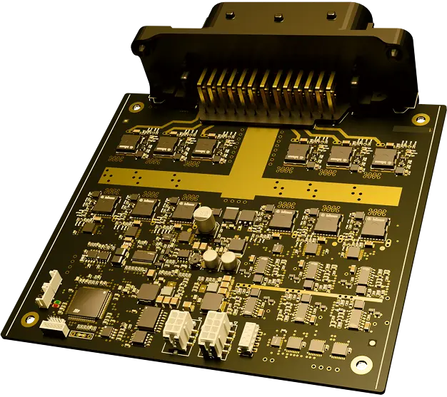
ELECTRONIC DEVICES FOR AIRPLANES AND CARS
X-ray analysis of electronic hardware

X-ray analysis of electronic hardware

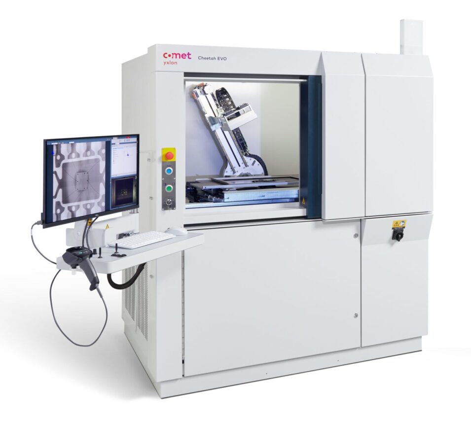
X-ray analysis is one of the most reliable ways to detect hidden defects in electronic components, solder joints and internal PCB structures that cannot be seen with the naked eye or microscope. AEV has a modern high-resolution X-ray system that allows for detailed inspection of even the finest structures in electronic assemblies.

Our X-ray laboratory provides services from quality control in serial production to detailed diagnostics of failures in prototypes and development samples. The result is the ability to quickly identify problems, reduce debugging time, increase electronics reliability and prevent failures in real operation.

For X-ray analysis, we use the modern YXLON Cheetah EVO system.

Precision X-ray inspection of electronic components and assemblies

Using a state-of-the-art X-ray system, we can examine the internal structure of electronic components without physically damaging them. X-ray inspection allows for:
  • detection of internal component defects
  • checking correct assembly
  • analysis of structural elements and internal details
  • verification of production and assembly quality
This type of inspection is essential for equipment where high reliability and long service life are required.

Inspection of solder joints – BGA, QFN and other packages

Modern electronics use a large number of components whose connections are hidden under the package and therefore cannot be checked by conventional methods. X-ray analysis allows for an accurate assessment of the quality of soldered connections, especially in:
  • BGA (Ball Grid Array)
  • QFN
  • CSP and other packages without accessible leads
  • Using X-rays, we detect:
  • voids (hollow spaces in the solder alloy)
  • cold joints
  • cracks
  • solder shortage or excess
  • shifts and deformations during the soldering process
This significantly increases production quality and eliminates potential failures in operation.

Detailed analysis of PCB and hidden layers

PCB X-ray inspection is invaluable in identifying damage that is invisible to the naked eye. We perform:
  • inspection of the inner layers of multilayer PCBs
  • verification of the integrity of conductive paths
  • detection of breaks, delamination or damage to the substrate
  • inspection of hidden connections and vias
This procedure is especially essential when developing prototypes, troubleshooting or verifying the quality of complex electronic assemblies.

ARE YOU INTERESTED IN THIS SERVICE?